|
|
MRS96 Fall |
|
|
|
|
[Presented at MRS'96 Fall Meeting, Boston,
November 1996] CROSS-SECTIONAL TRANSMISSION ELECTRON MICROSCOPY OF Si-BASED NANOSTRUCTURES MAXIM V. SIDOROV and DAVID J. SMITH* Center for Solid State Science, Arizona State University, Tempe AZ
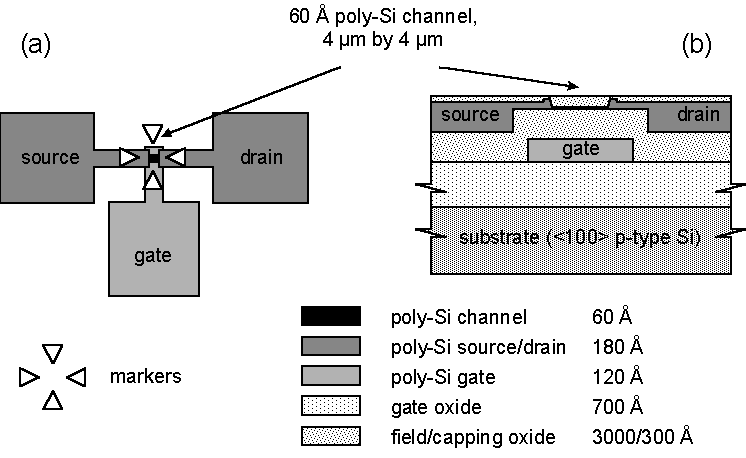
85287-1704 USA ABSTRACT This work demonstrates the successful application of the precision cross-sectioning technique to the characterization of two types of Si-based nanostructures. Careful wedge-polishing of an array of metal-coated poly-Si microlines gave electron transparency over areas as broad as 1.5 mm across. A single, specific, SET (Single Electron Transistor), having dimensions of 4 x 4 m2, was cross-sectioned for examination using conventional and high-resolution TEM imaging. INTRODUCTION Since the introduction of integrated circuits, the number of individual elements that can be placed upon a single chip has doubled approximately every three years: nowadays, this trend translates to multi-megabit DRAM memories with over 9 million elements per chip. Moreover, novel ways are continually being sought to allow reductions in device dimensions. This tendency creates great challenges for preparation techniques which can provide access to the volume to be analyzed. Although SEM (Scanning Electron Microscopy) is still the most commonly used technique for failure analysis, the much higher spatial resolution and image contrast available from TEM (Transmission Electron Microscopy) has motivated many research laboratories to use TEM for process development and failure analysis. Our current objective is to develop reliable procedures and protocols of precision sample preparation suitable for TEM characterization of nanoscale patterns and devices. Preparation of specimens for TEM is an integral part of, and precedes, the microscopy in all cases. The main objective is to produce a section (or ‘foil’) of material that is thin enough to be transparent to the electron beam and enabling the major microstructural features to be imaged. Even for traditional samples (bulk materials, continuous films and structures), specimen preparation via combinations of mechanical grinding/polishing and final thinning with a broad ion-beam requires certain skills and experience. When it comes to site-specific samples (small pre-defined features), specimen preparation can become a nightmare for a microscopist. It is frequently necessary to access a specific pre-defined volume of material having dimensions of 1 m3 or less. Traditional methods do not have sufficient precision and thus must be modified. In this paper we describe the application of recently developed precision sample preparation methods to Si-based sub-micron and nano-scale structures. EXPERIMENTAL Precision thinning methods were developed over the last several years by improving the accuracy of mechanical grinding and polishing [1-3]. These methods are mainly based upon the tool known as the Tripod Polisher [1] (developed at IBM in the late 1980’s). In our work we have applied a similar tool, known as the Precision Angle Lapper (PAL) [4]. This tool defines the polishing plane with three points: one point is the specimen being polished and the other two points are plastic legs driven by micrometers. The design of the tool allows for the precise adjustment of the position and inclination of the polishing plane (with better than 0.2 m and 0.2 mrad accuracy for position and angle respectively). The details of the sample preparation routine can be found elsewhere [1-3, 5,6]. In brief, the main preparation steps are: 1. Identification of the feature of interest;
8. (optional) Brief ion-milling from the second side (or both sides in the case of wedge-polishing) to remove mechanical damage and surface contamination. The micrographs presented here were obtained in a JEM 4000EX high-resolution electron microscope operating at 400 kV. APPLICATIONS Cross-sectioning of isolated microlines using wedge polishing The wedge polishing is accomplished with the tripod tool by introducing a small (~ 50 mrad) inclination of the polishing plane when the sample is polished from the second side. The wedge polishing technique is especially useful when applied to bulk materials, plan-view samples and cross-sections of relatively thick (> 1 m) films/structures. It also becomes useful if one wants to avoid ion-beam damage to a sample, since this technique allows samples suitable for TEM to be produced without ion-milling. When used with care, wedge polishing can yield impressive results, allowing very large electron-transparent areas to be produced. If not destroyed by fracture, the entire sample can be made electron transparent. This is in contrast to several microns at best, achievable with traditional methods. In our example, we have applied the wedge polishing technique to a continuous array of metal-coated poly-Si microlines (of various widths, ranging from 0.1 to 10 m) embedded into 2m-thick SiO2 layer on Si substrate. With dimensions of 5 by 2 mm, the array of lines was easily identifiable by optical microscopy and the sample was cross-sectioned perpendicular to the lines using a tripod polisher. At the final stage of the thinning process, a slight inclination of the polishing plane was introduced (toward the structure-side of the sample). The glass slide glued on top of the structure is used as a rough indicator of the specimen thickness as it starts to erode first. The polishing is stopped when the glass is all (or almost all) eroded away. The resulting TEM specimen had an electron-transparent area as large as 1.5 mm (with some dents and interruptions) along the Si/SiO2 interface. Figure 1a shows a 100 m long fragment of the structure containing 6 groups of lines. The line width decreases from group to group (the left-most group consists of 1m-wide lines, the right-most one is hardly visible at this magnification and consists of 0.2 m lines). Figure 1b shows a group of 0.6 m lines revealing a defect in the structure (pointed by arrow): a short-out between thin metal layers underneath a pair of neighboring lines. In some places, the specimen was thin enough for high-resolution TEM, as illustrated in Figures 1 c, d. [click on image to see a better (bigger) picture]
Figure 1. Cross-sectional TEM images of an array of isolated microlines. TEM sample was prepared using the wedge polishing technique without ion-milling. (a) Low magnification image of 100m-long fragment of the structure. (b) Higher magnification image of a group of 0.6m-wide lines. (c, d) High resolution images showing the Si/SiO2 and SiO2/metal/poly-Si interfaces. Cross-sectioning of the channel area of an individual Single Electron Transistor In this example, the precision methods of TEM sample preparation were successfully applied to obtain a cross-section of the channel area of a predefined thin film transistor. Schematic views of the device are presented in Figure 2. [click on image to see a better (bigger) picture]
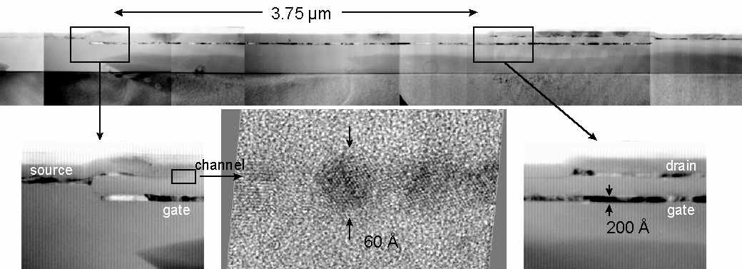
Figure 2. Schematic of single electron transistor: (a) top view, (b) expected cross-sectional view Since the transistor structure was only ~100 nm thick, it was not visible under an optical microscope when viewed edge-on. In order to allow for visual control during the cross-sectioning, the 4 by 4 m2 channel area was marked with four etched pointers penetrating deep into the substrate. The specimen was ground/polished from the first side until the cross-section plane reached the markers. After that, the specimen was ground/polished from the other side down to ~10 m thickness and mounted on a copper supporting washer. Conventional broad-beam ion-milling was used at the final stage of the thinning process. The milling (from the second side only) was frequently interrupted and the specimen checked under an optical microscope. The milling was stopped when thickness interference fringes started to appear (this occurs at thicknesses on the order of 1 m or less). Finally, the specimen was briefly ion-beam polished at reduced accelerating voltage from both sides. Figure 3 shows an overview of the entire channel area and enlargements (left and right) show key regions of the structure (source and drain layer edges). The high resolution image of the channel layer (bottom center) shows the polycrystalline nature of the Si-channel layer. [click on image to see a better (bigger) picture]
CONCLUSION It has been demonstrated that the novel precision methods of specimen preparation allow reliable access to very small, predefined Si-based nanostructures for TEM examination. Acknowledgments Special thanks to Jrn Ltzen and Greg Starr for providing the materials for the ongoing project. This work has been supported by ARPA through the office of Naval Research, grant N00014-95-1-0918. The electron microscopy was conducted at the Center for High Resolution Electron Microscopy at Arizona State University supported by NSF grant DMR-9314326. References
Last updated: April 28, 2017 |
|